SemiQon Cryo-CMOs
Cryo-optimized CMOS solutions to scale up quantum computing across qubit modalities
The world’s first CMOS technology fully optimized for cryogenic conditions. By integrating qubit control directly inside the cryostat we make quantum computers more scalable, efficient, and commercially viable.
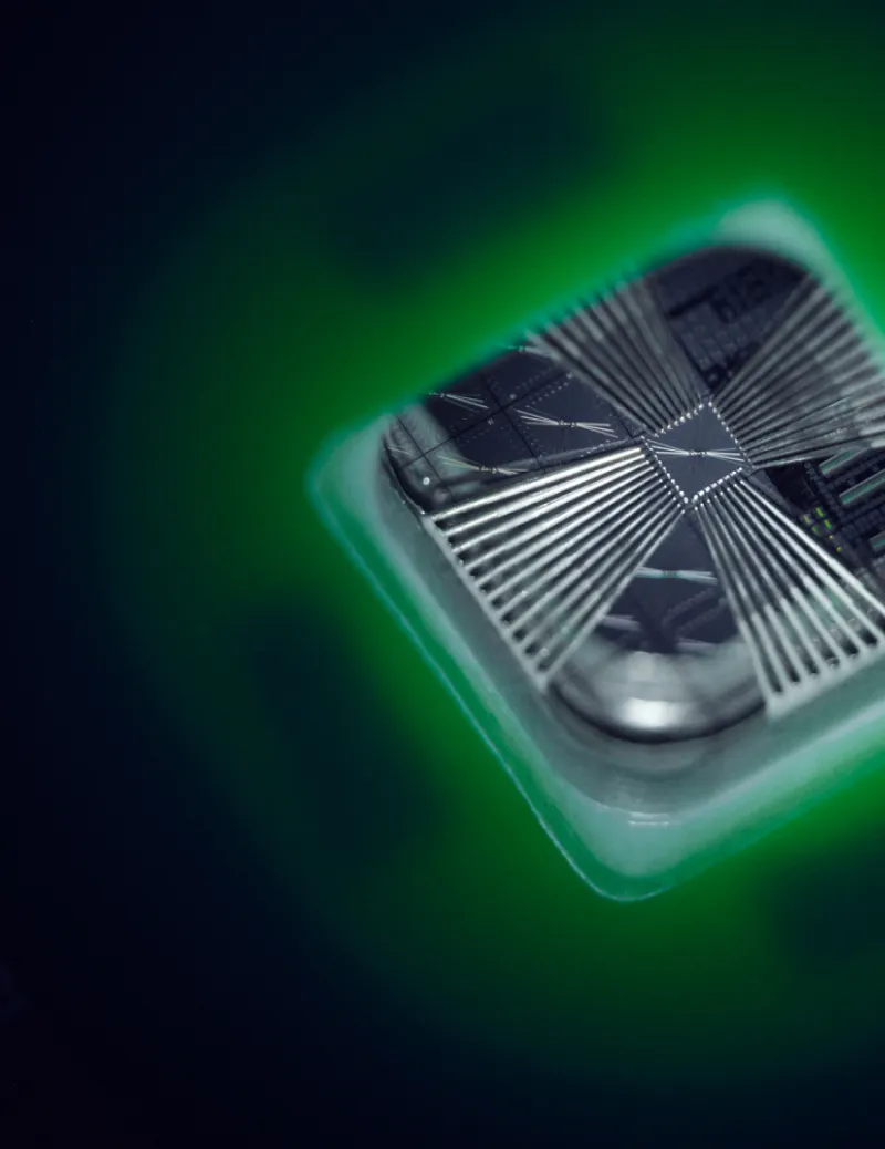
The Challenge
Breaking the bottlenecks in quantum hardware
Quantum computers are expanding, but to be commercially viable, they must become smaller, more efficient, and cost-effective. Today, control electronics remain one of the biggest bottlenecks limiting scalability and affordability.
Key challenges SemiQon's cryo-optimized CMOS addresses:
- I/O limitations: Room-temperature electronics increase the cost and complexity in quantum processor interfacing
- High power use: Traditional control electronics consume too much power and generate heat
- Lack of design kits: Cryogenic silicon IC development lacks standardized toolkits
- No integrated control solution: Until now, no practical approach has existed for qubit control via cryogenic silicon ICs
The solution
Our breakthrough: Cryo-optimized CMOS integrated with quantum processors
SemiQon’s ultra-low dissipation cryo-optimized CMOS technology integrates qubit control directly inside the cryostat. This eliminates the need for bulky, power-hungry room-temperature electronics and significantly reduces the infrastructure burden, making quantum systems less complex and more efficient to operate.
Our cryo-optimized CMOS is built to solve problems that are universal across qubit technologies. It is compatible with all major modalities, including superconducting qubits, semiconductor spin qubits, photonic qubits, and trapped-ion architectures that require cryogenic interfaces.
SemiQon’s cryo-optimized CMOS platform serves multiple electronics functions, available as RF switches, multiplexers, de-multiplexers, amplifiers, and memory elements.
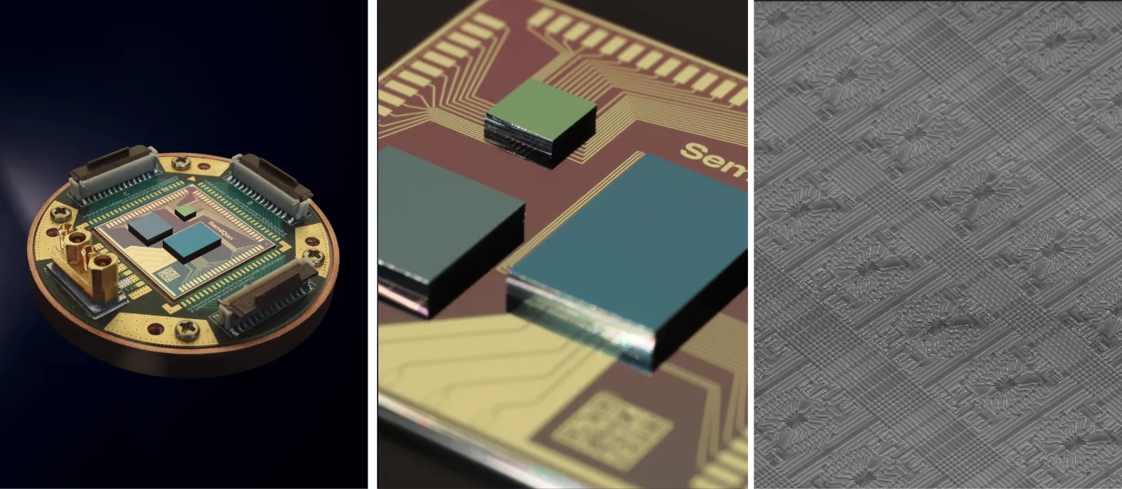
Packaged chip / Silicon die / Micrograph of CMOS device
Cryo-optimized CMOS RF switches
Building on our cryo-optimized CMOS platform, SemiQon RF switches bring signal routing inside the cryostat. Operating at the millikelvin stage, right next to the qubits, they direct control and readout signals on chip, so a single line from room temperature can address many qubits through a multiplexer tree. They run within the tight cooling budget of a dilution refrigerator, preserve weak readout signals through low insertion loss, and keep channels from interfering through high isolation.
The result: fewer cables, lower heat load, and a clear path to scale.
- Low heat load: operates within the tight cooling budget of a dilution refrigerator
- Low insertion loss: preserves weak readout signals
- High isolation: minimizes channel-to-channel crosstalk
- Compatibility: variants available across qubit modalities
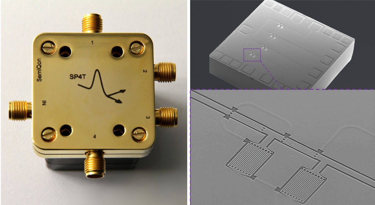
SemiQon's cryo-optimized CMOS
- 1000× lower power consumption than traditional control electronics
- 30% infrastructure cost reduction for quantum hardware manufacturers
- Cryogenic-ready 2.5D/3D packaging for seamless cold integration
- In-house manufacturing & fast iteration from pilot line to packaged device
- Delivered lab-ready & engineered to work
- World-first cryo-optimised CMOS transistor, delivering a clear first-mover advantage
- Modality-agnostic: compatible across qubit modalities
Where Cryo-CMOS makes a difference
Quantum computer makers & system Integrators
Simplify cryogenic control. Scale systems with less wiring, less heat, and less infrastructure.
Space electronics
Power cold-environment electronics in compact, efficient form factors. Potential uses in deep-space applications such as telescopes, Lunar and Mars exploration, and SNSPD.
High-performance computing (HPC)
Advance low-temperature logic with ultra-efficient silicon components optimised for dense architectures.
How are we different?
First-mover advantage
SemiQon has developed the world’s first CMOS transistor fully optimized for cryogenic operation
Built on silicon
Uses traditional CMOS (Si), avoiding exotic materials that require costly infrastructure
In-house manufacturing
Chips are developed in a semiconductor pilot line, enabling speed and quality control
Cryogenic packaging expertise
Our packaging is tailored for cryogenic performance and ready for immediate deployment
Strategic partner, not just a supplier
We collaborate closely with early adopters and integrate feedback into new designs
Modality-agnostic
SemiQon's cryo-optimized CMOS is a modality-agnostic platform, compatible with all major qubit technologies.
Technical specs
| Technology | Min. subthreshold swing swing (mV/dec) | Subthreshold gain increase (RT/cryo) | ION increase (cryo/RT) | Δ V t h (mV) | Source |
|---|---|---|---|---|---|
| SemiQon | 0.32 | 203 × | 10 × | Tunable | N. Yurttagül et al. https://arxiv.org/abs/2410.01077 (2024) |
| 14nm FinFET | 15 | 5 x | 6 x | 80 | A. Chabane et al., ESSCIRC 2021 – IEEE 47th European Solid State Circuits Conference (ESSCIRC), Grenoble, France, 2021, pp. 67-70. 10.1109/ESSCIRC53450.2021.9567802 |
| 28nm bulk CMOS | 20 | 4 x | - | 160 | A. Beckers, et al., 47th European Solid-State Device Research Conference (ESSDERC), 2017. 10.1109/ESSDERC.2017.8066592 |
| 28nm FDSOI | 5 | 14 x | 7 x | Tunable | B. C. Paz et al., 2020 IEEE Symposium on VLSI Technology, Honolulu, HI, USA, 2020, pp. 1–2. 10.1109/VLSITechnology18217.2020.9265034 |
| 40nm bulk CMOS | 28 | 3 x | 3.5 x | 120 | R. M. Incandela et al., IEEE J. Electron Devices Soc., vol. 6, 2018. 10.1109/JEDS.2018.2821763 |
| 160nm bulk CMOS | 23 | 4 x | 3 x | 150 | R. M. Incandela et al., IEEE J. Electron Devices Soc., vol. 6, 2018. 10.1109/JEDS.2018.2821763 |
| 22nm FDX | 14 | 5 x | 6 x | Tunable | O. Seidel et al., Fermi laboratory report for DoE, OSTI ID: 2217187. https://www.osti.gov/servlets/purl/2217187/ (2023) |
Seeking deeper technical insight into our cryogenic transistor design?
Read our peer-reviewed paper Millikelvin Si-MOSFETs for quantum electronics, published in Applied Physics Letters.
FAQs
What is cryo-CMOS?
Most electronics we use every day, from phones to data centers, are built on a technology called CMOS (complementary metal-oxide semiconductor). It is the standard way chips and transistors have been manufactured for decades.
Cryo-CMOS takes this same proven technology and redesigns it from the ground up to work in extremely low temperatures (known as cryogenic environments), typically at temperatures close to absolute zero.
This matters because systems like quantum computers need to operate at these temperatures, but the standard electronics used to control them were never designed for such conditions and waste too much power and generate too much heat when cooled down. SemiQon's cryo-CMOS solves this with dramatically lower power consumption and heat dissipation, designed specifically for cryogenic environments.
What temperatures does cryo-CMOS operate at?
Our cryo-CMOS transistors are engineered to perform optimally across a wide range, from the millikelvin regime up to 100 K. In our published research (Millikelvin Si-MOSFETs for Quantum Electronics), we characterized transistor performance at both 4.2 K and 420 mK, achieving a subthreshold swing of 0.32 mV/dec at the lower temperature. This means our electronics can serve both the higher-temperature stages of a dilution refrigerator, where control logic and signal chain components typically operate, and the sub-1 K stages closest to the qubits themselves.
How does SemiQon's cryo-optimized CMOS electronics compare to traditional transistors and other cryo-CMOS solutions?
Compared to conventional room-temperature transistors used in cryogenic environments, our cryo-CMOS transistors consume 0.1% of the power and dissipate 1,000× less heat. Unlike standard transistors that are simply cooled down and left to underperform, ours are built for cryogenic operation using a custom fully depleted silicon-on-insulator (FDSOI) process.
Our transistors achieve a minimum subthreshold swing of 0.32 mV/dec and a 203x subthreshold gain increase from room temperature to cryogenic operation, resulting in significantly lower power consumption and heat dissipation compared to other cryo-CMOS solutions. Our cryo-CMOS is fully compatible with standard CMOS processes, and with in-house design and fabrication, we maintain rapid development cycles and strong quality control.
Is SemiQon's cryo-CMOS technology compatible with different qubit types?
Yes. Our cryo-optimized CMOS electronics are designed as a modality-agnostic platform compatible with all major qubit technologies, including superconducting qubits, semiconductor spin qubits, photonic qubits, and trapped-ion architectures that require cryogenic interfaces.
Is cryo-CMOS only useful for quantum computing?
Any application that requires reliable, power-efficient electronics at extreme cold temperatures can benefit from our cryo-CMOS electronics. Space systems such as deep-space telescopes and planetary exploration hardware face similar cryogenic constraints, and high-performance computing architectures are exploring low-temperature operation for greater density and efficiency. We are currently exploring the space applications for our cryo-CMOS technology with support from the European Space Agency.
Why can't regular CMOS electronics be used at cryogenic temperatures?
Standard CMOS transistors were designed to operate at room temperature. When cooled to cryogenic conditions, they suffer from performance degradation including threshold voltage shifts, carrier freeze-out effects, and unpredictable behavior. They still technically function, but they underperform chronically, consuming far more power and generating far more heat than the cryogenic environment can tolerate at scale.
Commercial inquiries and partnerships
Yukihisa Tsuruta
Business Development Director
Featured News & Insights
.png)

The more we compute, the more heat we create. Now what?

Peter Sarlin-led PostScriptum invests in quantum hardware developer SemiQon
.png)
.png)